ASOS: “Hey, I know how they generate those numbers!”

The picture above is of one of the computers built into the ASOS array. I took one look at it and realized that I was looking at a bunch of 7-segment LED displays. “Hey!” I thought to myself. “I know how they do that!”

Indeed, that is exactly how they do it. A 7-segment LED is a 7-segment LED, regardless of whether it’s on a fancy machine, or made on a breadboard in a lab back in California:

7-segment display  7-segment display schematic

Knowledge is a wonderful thing!

binary counter breadboard

Preparing a PCB for assembly

PCB drilling with John

This will be a set of step-by-step, illustrated instructions on how to move from the software of a PCB (printed circuit board) to the point where you’re ready to assemble the components on it. It includes design of the stencil, etching, drilling and cleaning. I do this in part to show what I’m doing this summer, and in part as a reference for people who are preparing their PCBs for the first time.

  1. Transfer the design to stencil

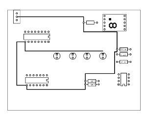
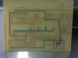
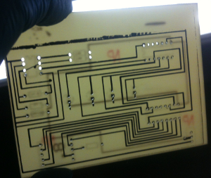
Most software produces a trace design that looks something like this (this was my design for a binary counting circuit from 0-15):

PCB final image

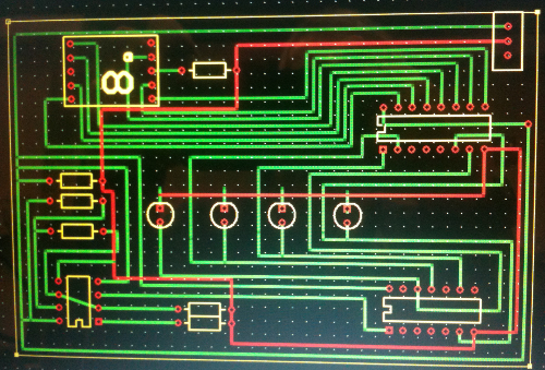
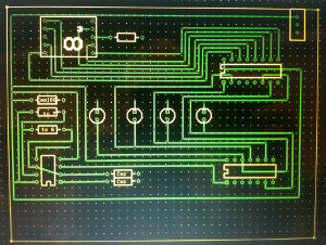
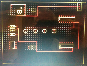
While pretty, it’s not usable because it has too much information. This design is for a 2-sided PCB. The red are the traces that will go on the top side, and the green are the traces on the bottom side. The yellow is the silkscreen layer, which you typically combine with the top side. Most programs will let you separate out the two sides with traces. Here are what mine look like:

PCB final bottom image   PCB final top layer image

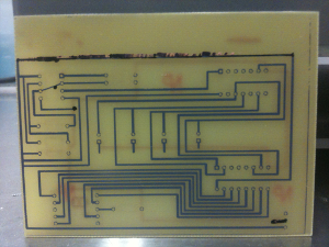
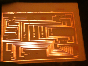
Once you get them to this point, you can print them to PDF with an appropriate driver. They will appear as black and white stencils, looking something like this:

PCB Top layer stencil PCB bottom layer stencil

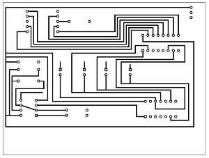
The stencils will mask the copper where it’s dark (those will be the traces and the pads) and will exposre the so that the etching solution can eat away the exposed copper layer and you will get nice traces where it’s masked.

  1. Clean the copper on the PCB

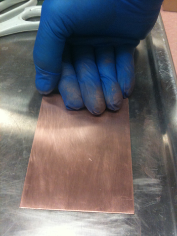
The problem with getting the stencil to stick to the copper plates is that the plates need to be really clean. So first we sand them with extremely fine sandpaper. You get a lot of copper dust; you can see it in the picture below on my gloves. We then wash the boards with acetone followed by isopropyl alcohol. In my day in the chem lab, isopropyl alcohol was just isopropyl alcohol. Now it’s known as IPA. For a moment I wondered why we were coating clean copper plate with a highly-hopped ale until I figured out that was a different IPA. As I often remind my students, context is everything.

PCB cleaned copper plate

  1. Press the stencils firmly onto the cleaned copper

You should already have trimmed the stencil to fit the board. Here’s what the cut-out stencils look like:

PCB blue sheets with copper plate

I used the lower right corner of the top side for my alignment, making sure I had a good fit and then ensuring that the back side lined up tightly with the top side, remembering that because you’ve flipped the plate over, you need to align it with the lower left side of the bottom plate.

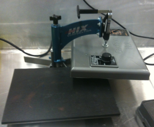
  1. Use the heat press to transfer the stencil

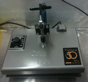
We found that heating the PCB in the heat press to 325° was about the right temperature for a good transfer. We also learned through sad experience that you have to lower the heat press very slowly so that you don’t blow the stencil paper off. Very, very slowly.  Then heat for 5 minutes. Below are pictures of the heat press, at left when it’s pressing down, and at right where you’ve swung the press to one side to insert your PCB and the stencils:

PCB heating press closed   PCB heating element open

  1. Fill in any gaps that the stencil didn’t cover

You should get a nice transfer, but occasionally you don’t. My outer power trace didn’t transfer too well. Sharpies to the rescue! It turns out that sharpies do a perfectly acceptable job of masking the copper from the etching solution. My outer power trace barely came through, so we darkened it with a Sharpie. I’d use a ruler next time, because the finally trace was more ragged than I’d like to appear. (It was far enough away from the other traces that it didn’t matter, but there were other traces where a ragged trace would have been disastrous.)

NOTE FOR PRINTMAKERS: the “etching” one does in preparing PCBs is actually the opposite for what’s done in fine-arts etching. There, the entire plate is covered, and the cover is scratched with an etching needle. The etching solution bites the plate where it’s exposed, and the ink is forced into the etched grooves and transferred to the paper. It’s like a photographic negative, for those of you who remember traditional photographic technology. The etching of a PCB is more like preparing a woodcut, linocut, or wood engraving, where the white space is cut away and the remaining part of the block on the surface gets the ink and makes a positive transfer to the paper. The PCB is similar, except that there’s no transfer, only the remaining trace after the rest of the copper has been eaten away by the etching solution.

Here’s what they look like after the heat press:

PCB stenciled plate top   PCB stenciled plate bottom

Note that the trace on the top right looks a little ragged. That’s where we drew more cover with the Sharpie by hand. Using a ruler would probably have resulted in straighter, neater-looking traces.

  1. Etch the plates

The masked PCB is placed in an etching solution, which will dissolve the thin layer of copper on the board where it’s exposed and will leave the masked sections as traces. It is more complicated than fine-arts etching, where eave the masked sections as traces. It is more complicated than fine-arts etching, where you only have to worry about biting (etcher’s term for etching) one side of the plate. Here, you are biting both sides of the plate, so you can’t simply put it on the bottom of a tray and cover it with etching solution. Instead, you have to expose it vertically.

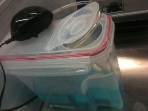
We used a t-frame that you can see in the picture below on the right. I don’t particularly like it, because the plate rests at an angle and is supported at places other than the edges. The t-frame can therefore cover parts of the plate where the copper is supposed to be dissolved. I think this design came about because it gave the etchers a place to hang and air hose to bubble water up through the etching solution. (In the picture at the right, you can see the aquarium pump (the black thing sitting on top of the tank cover.) If you don’t bubble air through the solution, bubbles can form where the etching solution dissolves the copper. Once a bubble forms, it prevents the etching solution from attacking and dissolving the copper as it’s supposed to do. Bubbling air through the solution pushes the bubbles off the plate and permits the etching to continue.

PCB etching tank side   PCB etching tank above

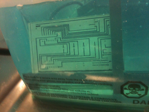
By the way, the blue color in the solution is typical of dissolved, oxidized copper. We use ammonium persulfate as the etching agent (not as fast as sulfuric, nitric, or hydrochloric acids, but it doesn’t have the nasty fumes that those acids do), so I’m assuming that we’re seeing a buildup of copper sulfate in the solution.

We typically etch PCBs for 30 minutes. It usually isn’t enough, and etch PCBs for 30 minutes. It usually isn’t enough, and you have to keep a very close watch on the etching solution from that time on. There were some copper smudge remaining on my PCB which took another 6 minutes to dissolve. I perhaps removed the plate a couple of minutes early, since there were other smudges that hadn’t been dissolved, as you can see in pictures below. However, I was more concerned about undercutting the traces if I didn’t remove the plate. (Undercutting is having the etching solution attack the masked traces from the side as it dissolves the unmasked copper. Some undercutting is inevitable. Indeed, if you leave a PCB in an etching solution for hours, you will probably have little copper remaining on the PCB. Once the etching solution has dissolved the unmasked parts of the PCB, it will attack the exposed sides of the traces and dissolve them. Vigilance is always necessary!

  1. Wash the PCB with water.

When the etching is finished, you have to wash the PCB really fast to make sure that you get the etching agent off. Otherwise, etching on your traces continues. Not a good thing!

PCB etched plate top  PCB etched plate bottom

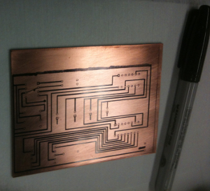
Again, you can see that the top trace on the bottom side (right-hand picture) is rather ragged. But there’s copper there, so practicality triumphs over aesthetics.

You could remove the mask at this time. However, the mask gives some protection to the surrounding copper for the next step: drilling.

  1. Drilling the holes for the components

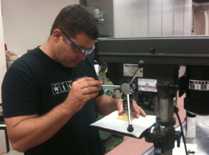
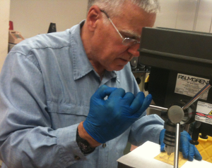
The PCB won’t work until you solder the resisters, capacitors, relays, integrated circuits, and all the other modern electronic wizardry that makes our age possible. To solder them on, you need to drill holes through the pads so the legs and prongs can fit through. Kits come with pre-drilled PCB. If you design your own circuits rather than using a kit, you have to drill them yourself. There’s a picture of John at the top of this entry drilling away. Same skills you used in wood shop or metal shop if your school had shop classes, except that the drill bits are really, really small.

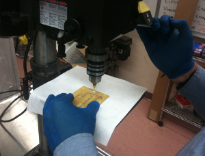
José took the following picture of me, which is one of many reasons I rarely post pictures of myself here. I was concentrating on the drilling, not on looking mean or mad. The picture on the right shows the drilling set-up, with a small pile of fiberglass dust where the hole was drilled:

PCB drilling JMH  PCB drilling from left

In the end, your holes should line up with the stencil:

PGB drilled circuit board bottom  PCB drilled circuit board top

  1. Remove the stencil.

You’re just about done, but you now have to remove the stencil. Go to the wet lab and remove the stencil, first with acetone, and then rinsing with isopropyl alcohol. Copper oxidizes really fast, which reduces conductivity, so if you’re not going to be soldering immediately, store your PCB in an airtight plastic bag until you’re ready to use it. Here is what the front and back of mine looked like after I was finished:

PCB cleaned trace top  PCB cleaned trace bottom


Next: soldering the components. (It will be a couple of weeks before I post anything on that, because I’ll be in Kansas City while my PCB is sitting in the lab in Pasadena.)

And now, for something completely different….

I have not been blogging this week because I’ve been finishing up part 1 at Cal Tech and preparing to leave tomorrow for Kansas City and the American Meteorological Society’s weather program at the National Weather Service Training Center. So be ready for a shift from electronics to weather! However, I have lots of pictures and other material to post, including a visit to Cal Tech’s clean rooms for nanofabrication, where the light is yellow and everyone wears protective gear to avoid contaminating the wafers being etched. The next few days, then, you’ll see a combination of the two different programs.

The title was the lead-in to the credits for the “Monty Python” television show. I haven’t posted much that’s funny (unless you consider volcanic eruptions, drought, and Common Core and Next Generation Science Standards to be side-splitters) of late, so here’s one of the great bits from Monty Python and the Holy Grail. King Arthur’s attempt to persuade the lord of the castle to join his quest for the Holy Grail runs afoul of the lord’s guard, who rightly accuses King Arthur of using coconuts to make the sounds of a galloping horse. King Arthur loses complete control of the conversation as the guard asks him where Arthur got the coconut, and then explains why a coconut could not possibly be present in England of that time. If there’s one example of something being “Pythonesque,” this is it.

Fun with Liquid Nitrogen

LN Melisa and Keith in the fog

Every science student sooner or later uses dry ice or its colder cousin, liquid nitrogen. Liquid nitrogen is increasingly coming into use because it’s really cold (-196°C [that’s -321°F!]) and because of its other good qualities. Aside from the cold, which can produce serious skin damage, liquid nitrogen is an ideal gas to use. It’s very difficult to get it to react with anything, and it’s not toxic (almost 80% of the atmosphere is made up of molecular nitrogen). Cal Tech uses so much of it that every lab has a dedicated nitrogen line where nitrogen gas is pumped in. Liquid N2 (sometimes abbreviated LN2) is available in large tanks. In fact, the tanks you see coming into our lab are liquid nitrogen tanks.

lab door 060

As we saw in the last post, we use nitrogen a lot for the high vacuum processes. We had a lot of fun learning how to use it safely. Here’s Keith demonstrating:

LN Keith demonstrating

There’s always a lot of water condensation (aka “fog”) when you pour it into a container.

LN Jose pouring LN2

We tried to pay homage to the Cal Tech Halloween tradition of throwing pumpkins frozen off of the Millikan library by freezing a glove to see if we could shatter it. No success, this time around:

LN glove after freezing

Here’s José, learning how to fill the dewar with LN2. Note the ideal gas law on the whiteboard at the right:

LN Jose with dewwar


Melisa also knows how extract LN2:

LN Melisa with LN2

Liquid nitrogen is useful in the lab and amusing to work with. Given how cold it is, I’m not sure I’d want it to be available in a K12 classroom.


Vacuum chambers and pumps

Vacuum chamber low vacuum

Much of the work in a nanofabrication lab takes place in vacuum conditions. Normal atmospheric pressure at sea level is about 760 torr, a fancy way of saying that normal atmospheric pressure can support a column of 760 mm of mercury (a little over 29 inches). Somebody somewhere along the way that it would be a Good Idea to substitute “torr” (after Evangelista Torrelli, the 18th century Italian scientist who invented the first barometer) for “mm of mercury.” I suppose it has the additional advantage of confusing the laity. Sigh.

Anyway, a normal vacuum pump can reduce the pressure from atmospheric pressure (760 torr) to about 10-2 torr. That’s more than 75,000 less pressure than the atmosphere provides at sea level. Pretty impressive, but not good enough for some of the work we do, that requires pressures of 10-6 torr.

At the top of the page is our normal vacuum chamber. We fired it up with a tied-off glove inside to see if we could pop it. We couldn’t, in part because there was so much silicone and epoxy polymers around the opening from 20 years of use that it wouldn’t hold a good seal. This vacuum chamber is used for epoxy molds, which often develop air bubbles. The easiest and most effective way of getting rid of air bubbles is to put it in a vacuum. Unhappily, it aerosolizes bits of the epoxy, which settle on the sides. All the pink you see inside the chamber? That’s not insulation, it’s the remnants of years and years of use. We’ll revisit this later in the week.

Often nanofabricators will want to deposit a very thin layer of metal on the top of another metal or a silicon wafer. Most metals melt at temperatures that are so high that doing it in an oven would melt the silicon substrate as well as the metal. The solution is to get the metal to boil at a lower temperature, where the gaseous metal can then be deposited in a thin layer on the silicon.

You can do the same thing with water and make it boil in a vacuum at room temperature. Here’s a quick demo on how that’s done:

Here’s a longer demo, with more explanation, but also with a thermometer, which shows you you’re at room temperature. Yes, you CAN make ice at room temperature, given a good enough vacuum and enough time.

What the metal-deposit systems add to the water demo is a heating element. They typically have a small crucible of tungsten, which has one of the highest melting points of all metals. The pressure is reduced so that most metals will boil at under 1,500°C. These very low pressures (counterintuitively called “high vacuums”) are achieved through a series of techniques to remove as much air and other gas as possible, which usually involves ionization and cooling oil droplets with liquid nitrogen.

Let me walk you through it. You put want you want coated in the chamber. Here are three pennies we coated with aluminum.

vacuum chamber high vacuum pennies to be coated

The aluminum was placed under the pennies in this “boat” made of titanium and melted once the pressure dropped.

vacuum chamber high vacuum titanium boat

Here’s the entire unit. The nitrogen trap is in the rear.

vacuum chamber high vacuum entire apparatus

Here’s Melisa filling the trap with liquid nitrogen.

vaccum chamber high vacuum melisa adding ln2

Under the bench, an ionizing light helps create the low pressures that make it relatively easy to boil metal.

vacuum chamber high vacuum ionization underneath

I don’t seem to have a picture of the aluminized pennies. I’ll ook for them and post another picture here if I can find them. Meanwhile, José has been doing an amazing job of fixing the pumps after years of heavy use and getting them up to standard.

Cal Tech Week 3: the high school students arrive

High school students arrive

On June 29, 2015, two high-school seniors from John Muir High School in Pasadena joined us. On the left is Melisa Herrera, and on the right is José Múñoz. Hopefully you recognize Keith Russell, Our Fearless Leader, in the background left, and John Smallenberg (in the Barça shirt) in the background left. They will be with us for the next 5 weeks.

Both Melisa and José are enthusiastic science students. After years of feeling like I had to pull teeth from science students to get them to concentrate, it’s a refreshing chance to work with the two of them. They are hard workers, willing to take on any task they are assigned, and are brimming with really good questions. They are a pleasure to have around.

José wants to be a mechanical engineer and wants to go to college at Cal Poly Pomona. Melisa isn’t entirely sure what she wants to study yet, but she knows it will be science, and is looking at college next year at Cal Poly San Luis Obispo.

Here’s another picture of them in front of the Gene Pool between Beckman Auditorium and the Beckman Institute. We were having monsoonal clouds (a high over the Great Basin was blowing the monsoonal moisture that usually travels up the Gulf of California into Arizona to California in the west) when I took the picture, which is why it’s as dark as it is.

High School students

Welcome Melisa and José!


Cal Tech Week 2, our second project: designing our own circuits with ICs

7-segment display

During our first week, we built a counter using a 7-segment display like that picture above. You’ve seen these digital displays everywhere. An IC sends an appropriate message to the 7-segment display, and the appropriate parts of the display light up. The circuit we built didn’t do things automatically…you need a timer chip for that….but it gave me an idea to build a binary counter with an analog, base-10 display.

clock_hands_spinning_clockwiseclock_hands_spinning_backward_md_wmThe reason for my interest in building a binary counter. When I started teaching, I realized that more than half of my students could only read time from a digital display. Standard analog clocks (see left) were mysteries to them. I immediately removed ALL digital clocks from my classroom, and put up mainly analog clocks, including one that ran backwards/counterclockwise (see right). The reason for the backward-running clock was based on my observation when I was teaching pre-calculus, which contains about a semester of trigonometry. Students struggled with the unit circle because they didn’t know the difference between clockwise and counterclockwise. So what better way to prepare students for trigonometry than to expose them to a backward-running clock?

The one exception I made to digital was a binary clock. Binary systems have only two digits, a 0 and a 1. It corresponds perfectly to electronics, which only know two numbers (on or off). It’s not particularly easy to teach, although once the students learn binary, they delight when adults come into the class and ask what the binary clock is and can explain it to them.

Here’s what a binary clock looks like.

binary wall clock

I have one just like this, except that I mount it on the wall. Below is a YouTube video that explains how to read binary clocks.

The problem in teaching binary is that binary clocks typically show time by flashing lights. Students often miss the connection between a specific binary number and its base-10 equivalent. If I could display both of them simultaneously, comprehension would be increased dramatically.

We already had the 7-segment circuit, so all I needed was a binary circuit. Keith had me google the web to look for a schematic, and we found one we could adapt easily with the ICs we had on hand. Here’s the circuit we chose, which I got from a website in the UK.

binary_counter circuit

We modified the design as we went along. Originally I had thought of doing a count-up and count-down timer, and maybe going up to 99 in base-10 (the maximum you could get out of 2 7-segment displays). Eventually, discretion proved again to be the better part of valor, and we decided to stay with a single 7-second display and 4 indicator lights, that would represent the 1’s, 2’s, 4’s and 8’s column, and count from 0 to 15 in base 10 (although we wouldn’t get a recognizable output for numbers 10 through 15 on the 7-segment display, although the binary counts would be OK.

Since this would eventually be transferred to a PCB, we needed to breadboard it first. It took a while to get everything attached correctly—schematics are really terrible in that they don’t correspond to the real geometry of the chips—but eventually we came up with a breadboard design that worked that looked like this:

binary counter breadboard

(I’ll be posting a link to a movie showing it in operation in a day or so.)

Eventually, however, we want to get this onto a PCB, which means a redesign of the circuit. From the breadboard, we at least knew what went where and why. But getting the trace to work correctly was a laborious process. I’m still not entirely there, though I expect this week to print the diagrams and etch the PCB. For now, here’s an intermediate diagram of the traces which should give you an idea of how things actually have to be laid out on a PCB.

binary counter intermediate trace design

Stay tuned for progress reports!

Soldering on

soldering practiceSoldering is necessary on any printed circuit board. We started practicing the first week with junked boards and burned-out components. It’s a good skill to have. I am concerned about what middle-school boys might do with soldering irons, but if you’re going to teach an electronics course, you have to teach the students how to solder.

soldering diagramIn theory, it’s simple. You put the components through the circuit board, flip it over, solder the piece in, and that’s that. There’s some skill to it, as you have to apply the soldering iron to both the wire and the joint to get enough solder to melt, and you need to leave the iron for a couple of seconds on the wire before removing it so the solder doesn’t harden prematurely. But it appears to be just about as simple as in the diagram.

This apparent simplicity, however, does not always survive contact with reality. To begin with you’re almost always soldering on the opposite side of the PCB from where the component is. This usually isn’t a problem when you’re starting out, as the board lies flat. But add a couple of electrolytic capacitors, and the component side won’t be flush against the lab bench. Gravity always wins, and your components can start to fall out.

soldering icsThere are other problems. Look at this picture. That’s an IC of some sort with 14 pins. Each pin has to be soldered in very carefully, and the solder has to be isolated from the solder on the adjacent pins. This can be a pretty nerve-wracking experience.

What’s also challenging is that you have your hands full, quite literally. One hand holds the soldering wire, and the other holds the soldering iron. What would be useful is to have a third hand in somewhere to push the component. A vice can sometimes help, though you still have the problem with gravity. Often you just need somebody else to come over and hold the component in place while you solder.

As the picture at the top of this page demonstrates, you don’t have to solder too many components in before you have a forest of wires sticking up on the bottom side of the board, and you can’t get at the next component you have to solder. The usual solution is to clip the wires as you go along. This works fine until you get a component in backwards, which is much more difficult to reinstall if the wires are clipped. Not impossible, mind you, but irritating in the extreme. On the other hand, you become a whole lot more careful so you don’t have to repeat the experience.

soldering then clippingWhat I’ve found the hardest about soldering are the connections for the ICs. Here’s my soldering on the back of either the transmitter or receiver unit. I got the soldering done well, but I was nervous while I did it. The solder had to be separate and not overlap onto an adjacent trace. These are really small components! I suspect you get better with a lot of practice. So the question is, how to we provide for that kind of time in a classroom where everything is oriented toward covering as broad a swath of material as possible and learn nothing in depth? Hmmm……

soldering

What’s a printed circuit board?

PCB top and bottom

Printed Circuit Boards (PCBs) have appear in earlier posts without my explaining exactly what they are. I hope this post remedies that omission.

PCB diagramPCB DIAGRAM. An electronic circuit isn’t much good unless it can be used. A functioning electronic circuit is typically mounted on a PCB. As this diagram illustrates, the PCB is typically an electrical insulator like fiberglass that has two copper faces on either side (you can also get one-sided PCBs). You draw out the diagram of where you want the wires to go, and etch the plate until the copper between them is eaten away and only the traces remain.

If you buy a kit, you’ll typically get the circuit board already prepared for you. Here’s an example of what a pre-packaged kit looks like:Printed Circuit-Board-Parts

You can see all the components (resistors, capacitors, and a few ICs, it looks like) and a board to mount them on. The PCB shows you what component goes where by the stencil that’s on top. All the holes you see are exactly that: holes leading through to the other side, where the traces transport the electrons around the circuit. You place the components in, solder them in place, and snip off the wires. Typically you’ll get a parts list and instructions on what to solder in where and in what order. As always, you have to be aware that some of the components have to be oriented in a specific way.

PCB topThis is more obvious on a simpler PCB like the one at the right. At the bottom of the PCB you can see a couple of circles with a “C1” inside the circle and a “+” next to one of the holes (note that they are different on each diagram. This is for an electrolytic capacitor. The legs of the capacitor passes through the holes. The “+” indicates that the positive leg must go through that hole. If you don’t assemble it correctly and have the negative leg where the positive leg should be, your circuit not only won’t work, but you might end up damaging the components.

PCB assembledWhen you’re done, the final board typically looks something like the picture at the left. (This is not the same board; I was looking for an image that was simple and clear enough.) The components sit on top on the fiberglass core, and the traces are on the back side. For those of you who remember desktop computers and swapped out “boards” in the back (e.g., for modems or SCSI ports), those “boards” were a typical example of PCBs.

All this is great if you have a kit. But what do you do if you’ve designed a circuit for which there is no kit? You make your own.

pcb unetchedIt’s easy and cheap to buy blank PCB boards. eBay and Amazon have them by the thousands, and they’re cheap. They aren’t much to look at, since they are nothing more than a piece of fiberboard with copper on one side or the other.

First, however, you have to design your traces. You would think that if you had a schematic, it would be simple. In fact, it’s annoyingly complex. It’s not at all uncommon, as we’ll see when I describe the binary counter circuit I’m building, that circuit designers run traces in that, if done literally, would result in short circuits. The schematic is just the beginning. I ended up going back and looking at my math texts on symmetry to try to get a handle on how to get all the traces working properly.

PCB stencilThere are good programs out there that will help you lay out the traces. Still, a lot of the work is trial and error, and I spent several days drawing traces out of ICs and doing strange things with them to get them aligned. (I’m sure with practice you get better.) When you’re done, you’ll have something that looks like the picture on the left. The straight lines are the traces; the holes are where the components go. (More on this later, as it’s another step you have to go through.)

Next, print out the design onto special transfer paper. This transfer paper is impressed onto the copper surface of the blank PCB with a heat press, and the trace lines stick to the surface. The paper is acid-resistant, so anything covered by the paper will be protected. Then, like a fine-art etching, you put the PCB in an acid bath. The unprotected areas of the copper surface are dissolved in the acid, and only the copper traces remain. This is the reverse of the typical etching process for art, where the acid bites lines into the plate, and you have to be careful that the protected lines are not underbit by the acid solution (in other words, don’t make thin lines in your trace diagram or you may not have any traces after the acid bath).

Two PCBs in an acid bath

Two PCBs in an acid bath

After the acid bath, the PCB is cleaned…and now begins the fun. Remember all those little holes in the diagram? That’s where the components stick in and have to go all the way through the board. All you have now is a location for them. Yes….you have to drill the holes yourself. Such are the pleasures of designing your own PCB.

Once the holes are drilled, the PCB should be ready for assembly. Occasionally you will lose a trace here and there. If it isn’t too extensive, you can paint in a trace with a silver pen, which acts like White-Out and provides a thin coat of silver to repair the broken or disappeared trace. From this point on, assembly is just like a PCB board, except that you’re sweating bullets to hope that everything lines up correctly. We’ll discuss the fun of soldering in the next post.